Building a BT macropad with the nRF52840Plus
Sep 24, 2026I was interested in working with BT and NFC so what better way to experiment than to make a small keyboard. In the last iteration of my adventure with keyboards, I routed a ATMEGA328P by myself with no status LEDS, way to debug anything besides tracing with a multimeter so I resolved to create a working circuit board this time with some more proper documentation.
Originally, I had started routing the RF chip antena myself but I found myself referring to the SEEED-XIAO schematic so I decided screw it, might as well use what they already had.
Hardware
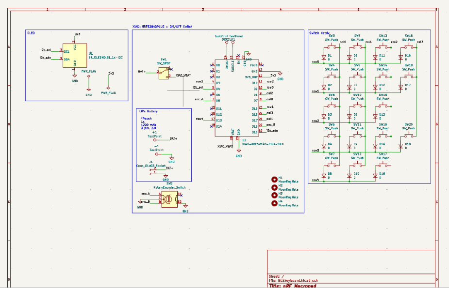
I decided on the SEED-XIAO nrf52840Plus for its adequate pins for my purpose, low quiscent current draw, and Bluetooth capability. The regular nrf52840 has too few pins for the key matrix rows and columns AND the SCL/SDA AND two extra EC11 pins. I did some quick google searches for the average Ah draw used by a keyboard for both on and off states and found a suitable LiPo and its JST2.0 connector.
Schematic
Peep the Test points
PCB Layout
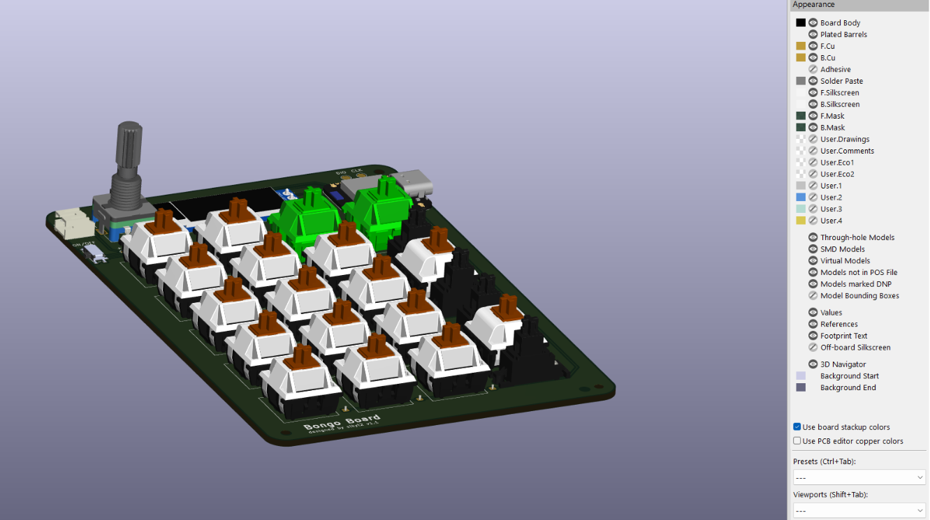
Routing was generally straightforward and I knew the layout I wanted already.
Assembly
I ended up soldering the castellated holes with solder paste and a hot plate sourced from the school. Thanks Chris!
Firmware
I decided on using the zmk software which is well supported for the Nordic line of semiconductors, Pro Micros, and most other keyboard enthusiast microcontroller boards.
It was relatively straightforward to get working. I flashed the uf2 made through github actions and then uploaded to the bootloader over the usb port on my computer. It took some time to figure out how to edit the synatactical xml sugar like the keymap, definitions, etc.
Problems
I could not get the rotary EC11 knob to work for some reason.
The quadrature pins were taken from an obscure forum but it showed significant instability in scrolling.
[WIP] Will need to use a logic analyzer and pinpoint this.
Takeaways and what I learned
- Sometimes paying a few more dollars for the non-cheap clone can be worth it.
- Always think about the physical orientation of parts. Retrospectively, I would have used pin headers for the nrf52840 instead of soldering it directly.
That’s all from me! See you next time